Owen's bridge is an ac circuit similar to Maxwell and Hay's bridge used for the measurement of self-inductance over a wide range of values. The principle of operation is similar to Maxwell and Hay's bridge i.e., balancing the loads on its four arms and comparing the unknown value with the known value. Here the unknown inductance to be determined is compared with the standard capacitor. Hence, it gives the value of self-inductance in terms of capacitance.
Construction of Owen’s Bridge :
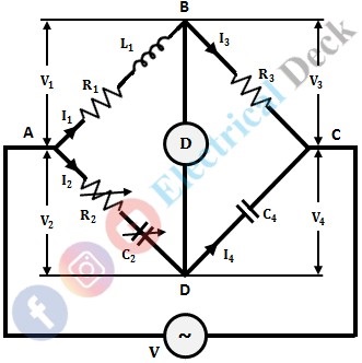
The circuit diagram of Owen's bridge for the measurement of inductance in terms of standard capacitance is shown in the figure below. It consists of an inductor in arm AB with inductance L1 and internal resistance R1 which is to be measured. A standard variable resistance and capacitance of R2 and C2 are placed in arm AD.
The arms BC and CD consist of standard resistance R4 and standard capacitance C4 respectively. A null indicator or detector is connected between junctions B and D, to balance the arms of the bridge.
Operation and Theory of Owen’s Bridge :
When the detector shows null deflection, it means the bridge is balanced. Since at balanced condition, the junctions B and D are at the same potential and no current flows through the detector. This can be done by varying the standard variable resistor R2 and capacitor C2 in arm AD.
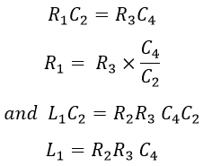
From the figure above, Under balanced condition, we have, Equating the real and imaginary terms on both sides, we get, Hence, the unknown inductor in arm AB is compared with the known capacitor in arm CD, and the value of inductance and internal resistance of the inductor are determined in terms of capacitance.
Phasor Diagram of Owen’s Bridge :
Let us draw the phasor diagram for Owen's bridge by using the relation between voltage drops and currents in each arm. Firstly, it should be noted that, across a resistance, the voltage and current through it are in the same phase.
Whereas in the case of the inductor and capacitor, the voltage leads the current by 90° and lags the current by 90° respectively. The phasor diagram of the bridge under balance conditions is shown below.
Taking current I1 as the reference phasor, as it is flowing in the arm AB. The voltage drop across R1 will be I1 R1 which lies in phase with I1. The voltage drop across the inductor will be I1 jωL1 which leads the current I1 by 90°. Thus, the total voltage drop V1 across arm AB will be the resultant of the sum of the drops across R1 and L1.
We know that when the bridge is balanced the junctions B and D will be at the same potential and no current flows through the null indicator, thus I1 = I3 and I2 = I4, also the drops V1 = V2 and V3 = V4. Hence, phasor V2 = V1. The drop V2 in arm AD is the sum of drops in resistor R2 and capacitor C2 i.e., I2 R2 + I2/jωC2.
Now the voltage drop V3 in arm BC i.e., in resistor R3, is I3 R3. Since I3 will be equal to I1 in the balance condition, thus the drop I3 R3 will lie along with I1. Also, V3 = V4 under balance condition, hence the drop V4 (i.e., I4/jωC4) will be same as V3.
The supply voltage V is the sum of drops V1 + V3 or V2 + V4. Therefore, the resultant of phasor V1 and V3 or V2 and V4 gives the supply voltage V.


